
在电子硬件研发领域,EDA(电子设计自动化)是连接创意与量产的核心工具。我记得N年前有在嘉立创打样过BMS样机的PCB,也买过物料,还买过假货,但在2026年的今天,抱着试试的态度使用了一下嘉立创的EDA工具,体验感还行。
长期以来,高端 EDA 市场被海外巨头垄断,不仅价格高昂、学习门槛高,还存在数据安全与供应链风险。嘉立创 EDA 作为完全自主知识产权的国产 EDA 工具,凭借云端化、全链路协同、低成本易用的优势,已成为 500万 + 工程师的首选,真正实现 “设计即制造、所设即可产”。

备注: 图1-仅用于练习试用的案例,如有错误等请忽略。
本文从核心功能、解决的行业痛点、全链路价值三个维度,全面解析嘉立创 EDA 如何成为硬件研发的 “国产生产力引擎”。
一、嘉立创 EDA:全栈式功能矩阵,覆盖设计全流程
嘉立创 EDA 提供标准版、专业版、教育版、私有化部署版,适配个人、团队、企业、高校等全场景需求,核心功能覆盖原理图设计、PCB 设计、仿真、库管理、协同、制造联动六大模块。
1. 原理图设计:高效、规范、可复用
-
超大工程支撑:支持 300 + 页、5 万 + 器件的复杂原理图设计,满足工业级、消费级多模块系统设计嘉立创EDA。
-
百万级元件库:内置 400 万 + 免费元件库,直接关联立创商城,实时同步库存、价格、规格书,无需手动建库、封装匹配嘉立创EDA。
-
模块化设计:支持电路模块复用,一键导入常用模块(如电源、通信、MCU 最小系统),大幅减少重复工作嘉立创EDA。
-
智能交互:WebGL 引擎驱动,拖拽式操作、自动连线、错误实时提示,新手 2 小时即可上手。
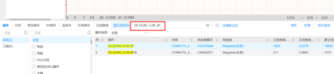
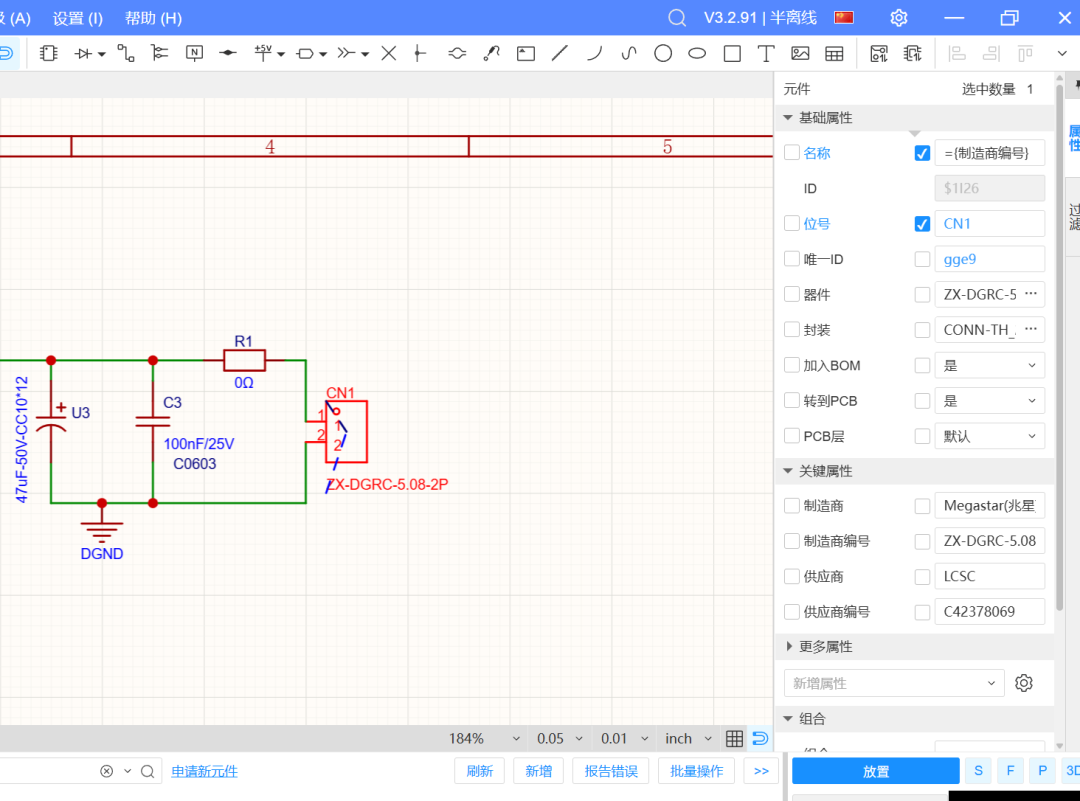
带出元件库和封装库
2. PCB 设计:专业、流畅、制造友好
-
高性能布线引擎:交互式布线、自动布线、推挤避让,支持 3 万 + 器件 / 10 万 + 焊盘的超大 PCB,多层板(最高 32 层)、盲埋孔、缝合孔一键操作嘉立创EDA。
-
2D/3D 实时预览:在线 3D 查看 PCB 与元器件装配效果,提前校验结构干涉、高度冲突,避免打样返工。
-
DFM 可制造性分析:内置嘉立创工厂制造规则,自动检查线宽、孔径、丝印、焊盘间距,一键定位问题并修正。
-
结构与面板设计:支持 PCB 拼板、挖槽、异形板设计,适配外壳装配与批量生产需求。

layout完成可下单
3. 协同与工程管理:团队研发的 “数字中枢”
云端实时协同:多人同时编辑同一工程,设计进度自动同步,告别文件传输、版本混乱。
统一中央库:企业版支持器件库、封装库、模块库集中管控,统一标准、避免重复建库,沉淀组织资产。
版本管理与追溯:工程自动存档、版本对比、修改记录可查,适配研发流程与质量管控嘉立创EDA。
跨平台兼容:浏览器直接运行(Windows/Mac/Linux),无需安装,随时随地设计。

4. 制造联动:设计到量产的 “最后一公里”
一键下单:设计完成后直接推送至嘉立创,PCB 打样、SMT 贴片、元器件采购、3D 打印一站式完成。
数据无缝衔接:无需导出 Gerber、BOM 手动核对,平台自动完成文件转换与生产校验,缩短周期 40%+。
成本透明可控:设计阶段即可查看制板、贴片价格,小批量打样成本降低 35%,工程变更响应≤24 小时。

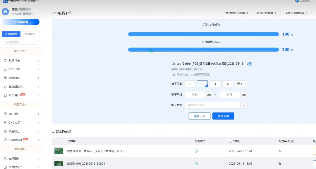
备注:元器件、PCB、SMT订单都可以下单。
二、嘉立创 EDA 解决了哪些行业痛点?
传统 EDA 与硬件研发流程存在高成本、高门槛、协同难、制造割裂、安全风险五大痛点,嘉立创 EDA 从根源上逐一破解。
1. 破解 “高成本”:免费 + 低价,降低研发门槛
永久免费:标准版永久免费,专业版年费仅为海外同类工具的 1/5,中小企业、个人、学生零成本使用。
打样补贴:每月提供免费 PCB 打样机会,大幅降低原型验证成本。
全链路省钱:设计 - 制造一体化,减少文件转换、人工校验、返工成本,整体研发成本降低 50%+。
2. 破解 “高门槛”:简单易用,快速上手
零安装、云端化:打开浏览器即用,无需配置环境、无需高性能电脑。
渐进式学习:新手引导、智能提示、海量开源工程,新手 1 周可完成从设计到打样,学习成本降低 60%。
中文界面 + 本土化服务:全中文操作、国内服务器、社区支持,告别语言与访问障碍。
3. 破解 “协同难”:云端协同,团队高效协作
解决异地办公、多角色协作的文件同步、版本冲突问题,多人实时编辑,研发周期缩短 30%+。
企业版支持权限管理、项目分组、资产沉淀,从 “个人画图” 升级为 “组织研发”。
4. 破解 “设计 - 制造割裂”:所见即所得,所设即可产
传统流程:设计→导出文件→人工校验→DFM 检查→修改→打样,周期长、返工率高。
嘉立创模式:设计阶段内置制造规则,3D 预览 + DFM 自动检查,设计完成直接下单,零返工、快交付。
5. 破解 “安全与自主”:国产自研,数据可控
100% 自主知识产权,无海外授权风险、无后门隐患,数据存储国内,适配信创与安全合规要求。
支持私有化部署,企业数据完全自主掌控。
三、嘉立创 EDA 的核心价值:从工具到生态,重构硬件研发
嘉立创 EDA 不只是一款设计软件,更是 **“设计 - 供应链 - 制造” 一体化生态 **,为硬件创新提供全链路支撑。
1. 对个人 / 学生:快速实现创意,低成本验证
-
零基础快速入门,海量开源项目参考,从想法到 PCB 样品仅需 1 周。
-
免费工具 + 免费打样,学生、创客零成本启动项目。
-
2. 对中小企业:降本增效,快速迭代
-
无需采购高价 EDA,节省软件成本;设计制造一体化,缩短研发周期,快速响应市场。
-
小批量灵活生产,适配新品试产、定制化需求。
3. 对大型企业 / 科研机构:安全可控,规模化研发
-
私有化部署 + 统一库管理,保障数据安全与研发规范。
-
多人协同 + 版本管控,支撑复杂项目与团队协作。
-
适配高多层板、高速信号、工业控制等高端设计需求。
-
4. 对教育领域:国产 EDA 人才培养基地
-
教育版免费授权,高校电子、自动化、物联网专业教学首选。
-
理论 + 实践结合,学生在校即可掌握工业级设计工具,无缝对接产业需求。
四、结语:国产 EDA 的崛起,硬件创新的新引擎
-
在国产替代与硬件创新的浪潮下,嘉立创 EDA 以自主可控、云端协同、全链路打通、低成本易用的核心优势,打破海外 EDA 垄断,成为 533 万工程师的共同选择。
-
从原理图到 PCB,从设计到量产,嘉立创 EDA 让硬件研发更简单、更高效、更安全。无论是个人创客、中小企业,还是大型企业与高校,都能在嘉立创 EDA 生态中找到适合自己的解决方案。
-
选择嘉立创 EDA,就是选择国产自主、选择全链路效率、选择更低成本的硬件创新之路。
备注:本文只是介绍一下国产EDA工具,不推销产品,仅推荐一款可替代进口EDA工具,作为一种备选,说不定在哪一天可以转正使用,作为辛苦的千万级硬件工程师和应届大学生、或者高中生等练手的一个福利推荐;

In the field of electronic hardware R&D, EDA (Electronic Design Automation) is the core tool connecting creativity and mass production. I remember years ago I had prototype BMS PCBs made at JLC and also bought components there, even some counterfeit ones, but today in 2026, I tried JLC's EDA tool with a tentative attitude, and the experience was decent.
For a long time, the high-end EDA market has been monopolized by overseas giants, with high prices, steep learning curves, and risks in data security and supply chain. As a domestic EDA tool with fully independent intellectual property rights, JLC EDA has become the first choice for over 5 million engineers by leveraging cloud-based, full-chain collaboration, low cost, and ease of use, truly realizing "design equals manufacturing; what is designed can be produced."
Note: Figure 1 is only a case used for practice; please ignore any errors.
This article comprehensively analyzes how JLC EDA has become a "domestic productivity engine" for hardware R&D from three dimensions: core functions, solved industry pain points, and full-chain value.
I. JLC EDA: A Full-Stack Functional Matrix Covering the Entire Design Process
JLC EDA offers Standard Edition, Professional Edition, Education Edition, and Private Deployment Edition, adapting to all scenarios including individuals, teams, enterprises, and universities. Its core functions cover six modules: schematic design, PCB design, simulation, library management, collaboration, and manufacturing linkage.
1. Schematic Design: Efficient, Standardized, and Reusable
Ultra-large project support: supports complex schematic design with 300+ pages and 50,000+ components, meeting industrial-grade and consumer-grade multi-module system design requirements for JLC EDA.
Million-level component library: built-in 4 million+ free component library, directly linked to LCSC, with real-time synchronization of inventory, prices, and datasheets; no need for manual library creation or package matching in JLC EDA.
Modular design: supports reuse of circuit modules, one-click import of common modules (such as power, communication, MCU minimal systems), greatly reducing repetitive work in JLC EDA.
Smart interaction: driven by the WebGL engine, with drag-and-drop operation, automatic wiring, and real-time error prompts; beginners can get started in 2 hours.
Component library and footprint library brought out
2. PCB Design: Professional, Smooth, and Manufacturing-Friendly
High-performance routing engine: interactive routing, auto-routing, push/shove and obstacle avoidance; supports ultra-large PCBs with 30,000+ components / 100,000+ pads, multi-layer boards (up to 32 layers), blind/buried vias, and stitch vias with one-click operation in JLC EDA.
2D/3D real-time preview: online 3D viewing of PCB and component assembly effects, early verification of structural interference and height conflicts to avoid prototype rework.
DFM manufacturability analysis: built-in JLC factory manufacturing rules, automatically checking line width, hole size, silkscreen, and pad spacing; one-click locating and fixing of issues.
Structure and panel design: supports PCB panelization, slot milling, and irregular-shaped board design, adapted to enclosure assembly and batch production needs.
Once layout is complete, you can place an order
3. Collaboration and Engineering Management: The "Digital Hub" for Team R&D
Real-time cloud collaboration: multiple people edit the same project simultaneously, design progress syncs automatically, eliminating file transfers and version confusion.
Unified central library: the enterprise version supports centralized management of component libraries, footprint libraries, and module libraries, unifying standards, avoiding duplicate library creation, and accumulating organizational assets.
Version management and traceability: automatic project archiving, version comparison, and modification history query, adapted to R&D processes and quality control in JLC EDA.
Cross-platform compatibility: runs directly in the browser (Windows/Mac/Linux), no installation required, design anytime and anywhere.
4. Manufacturing Linkage: The "Last Mile" from Design to Mass Production
One-click ordering: after design is completed, push directly to JLC; PCB prototyping, SMT assembly, component procurement, and 3D printing are completed in one stop.
Seamless data handoff: no need to manually export Gerber or verify BOM; the platform automatically completes file conversion and production validation, shortening cycle time by 40%+.
Transparent and controllable costs: PCB fabrication and SMT pricing can be viewed at the design stage; small-batch prototyping costs are reduced by 35%; engineering change response time ≤ 24 hours.
Note: Orders for components, PCB, and SMT can all be placed.
II. What Industry Pain Points Does JLC EDA Solve?
Traditional EDA and hardware R&D processes have five major pain points: high cost, high barrier, difficult collaboration, disconnected manufacturing, and security risks. JLC EDA cracks them one by one at the root.
1. Cracking "High Cost": Free + Low Price, Lowering R&D Barriers
Permanently free: the Standard Edition is free forever; the Professional Edition annual fee is only 1/5 of similar overseas tools. SMEs, individuals, and students can use it at zero cost.
Prototype subsidy: free PCB prototyping opportunities are provided monthly, greatly reducing prototype verification costs.
Full-chain savings: integrated design-to-manufacturing reduces file conversion, manual verification, and rework costs, lowering overall R&D costs by 50%+.
2. Cracking "High Barrier": Simple and Easy to Use, Quick to Learn
Zero installation, cloud-based: open the browser and use it directly; no environment configuration or high-performance computer needed.
Progressive learning: beginner guidance, smart hints, and a wealth of open-source projects; beginners can go from design to prototyping within one week, reducing learning costs by 60%.
Chinese interface + localized services: full Chinese operation, domestic servers, and community support, eliminating language and access barriers.
3. Cracking "Difficult Collaboration": Cloud Collaboration for Efficient Teamwork
Solves file synchronization and version conflict issues in remote office and multi-role collaboration; multiple people edit in real time, shortening R&D cycles by 30%+.
The enterprise version supports permission management, project grouping, and asset accumulation, upgrading from "individual drawing" to "organizational R&D."
4. Cracking "Design-Manufacturing Disconnection": What You See Is What You Get; What Is Designed Can Be Produced
Traditional process: design → export files → manual verification → DFM inspection → modification → prototyping, with long cycles and high rework rates.
JLC model: manufacturing rules are embedded at the design stage, 3D preview + DFM automatic inspection, and orders can be placed directly after design; zero rework and fast delivery.
5. Cracking "Security and Independence": Domestic Self-Developed, Data Controllable
100% independent intellectual property rights, no overseas licensing risk, no backdoor risks; data stored domestically, compatible with Xinchuang (domestic IT innovation) and security compliance requirements.
Supports private deployment, allowing enterprises to fully control their own data.
III. Core Value of JLC EDA: From Tool to Ecosystem, Reconstructing Hardware R&D
JLC EDA is not just design software; it is an integrated ecosystem of "design - supply chain - manufacturing," providing full-chain support for hardware innovation.
1. For Individuals/Students: Quickly Realize Ideas, Validate at Low Cost
Beginners can get started quickly, with a wealth of open-source project references; from idea to PCB sample in just one week.
Free tool + free prototyping; students and makers can start projects at zero cost.
2. For SMEs: Reduce Costs and Increase Efficiency, Rapid Iteration
No need to purchase expensive EDA software, saving software costs; integrated design and manufacturing shortens R&D cycles and enables rapid market response.
Flexible small-batch production, adapted to new product trial production and customization needs.
3. For Large Enterprises / Research Institutions: Safe, Controllable, and Scalable R&D
Private deployment + unified library management ensures data security and R&D standards.
Multi-person collaboration + version control supports complex projects and team collaboration.
Adapts to high multi-layer boards, high-speed signals, industrial control, and other high-end design needs.
4. For Education: A Base for Cultivating Domestic EDA Talent
The Education Edition is free for authorized use and is the first choice for teaching in university electronics, automation, and IoT programs.
Combining theory and practice, students can master industrial-grade design tools while still in school, seamlessly connecting to industry needs.
IV. Conclusion: The Rise of Domestic EDA, a New Engine for Hardware Innovation
In the wave of domestic substitution and hardware innovation, JLC EDA, with its core advantages of independent controllability, cloud collaboration, full-chain connectivity, low cost, and ease of use, breaks the overseas EDA monopoly and has become the shared choice of 5.33 million engineers.
From schematic to PCB, from design to mass production, JLC EDA makes hardware R&D simpler, more efficient, and safer. Whether individual makers, SMEs, or large enterprises and universities, all can find a suitable solution in the JLC EDA ecosystem.
Choosing JLC EDA means choosing domestic independence, full-chain efficiency, and a lower-cost path to hardware innovation.
Note: This article only introduces a domestic EDA tool and does not promote any product. It merely recommends an alternative to imported EDA tools as an option. Who knows, one day it may become fully adopted. It is a benefit recommendation for the tens of millions of hardworking hardware engineers, fresh graduates, or even high school students to practice with.
Download address: https://lceda.cn/