
智能手环频繁充电、无线传感器换电池麻烦、蓝牙智能设备无故断电断联,无线设备的核心痛点,始终绕不开「续航」二字。
在蓝牙芯片、无线射频芯片赛道,Nordic产品一直是低功耗领域的热门选择。不少开发者实测,同场景、同电池容量下,搭载 Nordic芯片的设备,续航时长比同类方案提升 40%-60%,核心功耗参数甚至能做到同类产品的 50% 左右。很多人会问:同是蓝牙射频芯片,为什么 Nordic 能把功耗压得这么低?
很多人对低功耗的理解,停留在“硬降电流”,但对蓝牙芯片、无线射频芯片而言,单纯拉低电流只会牺牲射频性能与连接稳定性。Nordic 的低功耗优势,本质是从硬件架构、射频前端,到软件协议栈、电源管理的全链路精细化设计 —— 不是靠 “节流” 硬砍功耗,而是靠精准调度,让芯片的每一分电量都用在刀刃上。

Nordic 全系列蓝牙芯片、无线射频芯片,均采用分层独立的电源域设计,内核、射频、外设、RAM 均配有独立电源开关,闲置模块可完全关断,杜绝微安级漏电流,同时支持多级睡眠模式,可根据场景灵活配置。
根据 Nordic 官方规格书,主流 nRF52832 芯片 System OFF 模式静态电流低至 0.3μA,深度睡眠下保持 RTC 运行 + RAM 数据保留仅需 0.6μA;而同规格同类芯片同模式静态电流普遍在 1μA 以上,待机功耗差距达 2-3 倍。针对复杂场景,nRF5340 等芯片采用双核异构架构,专用网络核负责射频与协议栈处理,无需唤醒应用核即可独立工作,应用核仅处理复杂任务时唤醒,避免大内核长期待机的无效功耗。

射频收发是芯片的功耗大户,也是 Nordic 的优化核心。其优化的低中频射频架构,让 nRF52832 芯片在 0dBm 发射功率下,DC/DC 模式典型发射电流仅 5.3mA、接收电流仅 5.4mA,+4dBm 发射功率下也仅 7.5mA;而同规格同类芯片同功率下工作电流普遍在 8mA 以上,收发功耗差距接近一半
同时,射频前端支持微秒级快速启停,从深度睡眠到完成射频收发仅需几微秒,让射频模块 “用完就睡”,无多余待机功耗。搭配优化的自适应跳频算法,可在 2.4GHz 同频干扰环境下,无需拉高发射功率即可保持稳定通信,间接降低功耗。
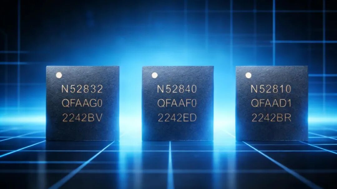
硬件是功耗基础,软件则决定了最终落地的功耗表现。Nordic 迭代多年的蓝牙协议栈与 nRF Connect SDK,采用全事件驱动调度逻辑,蓝牙广播、连接等基础操作可在底层完成,无需频繁唤醒应用内核,让芯片长时间停留在深度睡眠状态。
开发者仅需简单配置即可开启自动休眠功能,无需手动处理复杂的电源管理逻辑,同时针对多协议并发场景做了专属调度优化,避免协议栈冲突导致的功耗飙升。
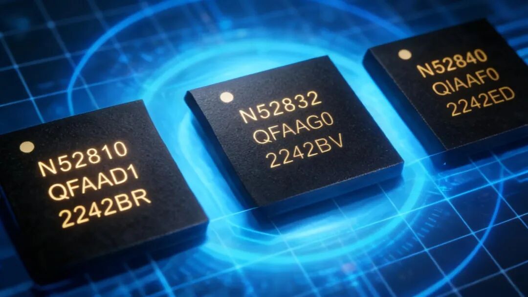
1. 入门低功耗场景(传感、简单蓝牙外设):nRF52810
2. 通用中端场景(可穿戴、智能家居):nRF52832
3. 高端多功能场景(多协议网关、工业传感):nRF52840
4. 新一代极致低功耗需求:nRF54L 系列
以上就是 Nordic 蓝牙芯片、无线射频芯片的低功耗核心逻辑。
Smart wristbands require frequent charging, wireless sensors need battery replacements, and Bluetooth devices unexpectedly lose power or connectivity. The core issue for wireless devices always comes down to "battery life."
In the field of Bluetooth and wireless RF chips, Nordic products are highly regarded for their low power consumption. Many developers have reported that, under the same conditions and with the same battery capacity, devices using Nordic chips last 40% to 60% longer than similar products. The core power consumption parameters are often only about 50% of those of competitors. So, why can Nordic suppress power consumption so effectively?
Many people think of low power consumption as simply reducing current, but for Bluetooth and wireless chips, this usually sacrifices RF performance and connection stability. Nordic's low power consumption advantage is based on meticulous design across hardware architecture, RF front-end, software protocol stacks, and power management. It's not about brute-force cutting power, but precise scheduling to ensure every bit of energy is used efficiently.
Hardware Foundations: Eliminating Unnecessary Power Loss
All Nordic Bluetooth and wireless RF chips feature a layered, independent power domain design. The core, RF, peripherals, and RAM each have their own power switches, allowing unused modules to be fully shut off and preventing microamp-level leakage currents. The chips also support multiple sleep modes for flexible configuration.
According to official specifications, the popular nRF52832 chipset has a static current as low as 0.3 µA in System OFF mode, rising to only 0.6 µA in deep sleep while maintaining the RTC and RAM data. In comparison, similar chips typically have static currents of 1 µA or more, meaning a standby power difference of 2 to 3 times. For complex scenarios, the nRF5340 uses a dual-core heterogenous architecture where a dedicated network core handles RF and protocol processing, allowing the application core to sleep and wake only when needed, thus avoiding the power drain of a large core running all the time.
RF Front-End: Minimizing Transmit and Receive Power
The RF section is a major consumer of power, and Nordic has optimized it extensively. The nRF52832's low-intermediate frequency architecture allows it to operate with a typical transmit current of 5.3 mA (DC/DC mode) at 0 dBm and a receive current of 5.4 mA. Even at +4 dBm, the current is only 7.5 mA. Similar chips typically require 8 mA or more for the same power levels, indicating a nearly 50% reduction in transmit/receive power.
Additionally, the RF front-end supports rapid microsecond-scale startup and shutdown, allowing the chip to enter deep sleep immediately after communication is finished, eliminating unnecessary idle power consumption. The optimized adaptive frequency hopping algorithm ensures stable communication without increasing transmit power in noisy environments.
Software Optimization: Simplifying Low-Power Implementation
While hardware sets the limits, software determines real-world performance. Nordic's Bluetooth protocol stack and nRF Connect SDK use event-driven scheduling, allowing Bluetooth advertisements and connections to be handled at the lowest level without waking the main application core frequently, keeping the chip in deep sleep most of the time.
Developers can easily enable auto-sleep functionality without needing to write complex power management code. The SDK also includes specific optimizations for multi-protocol scenarios, preventing power spikes caused by stack conflicts.
Recommended Chipsets for Different Scenarios
1. Entry-level low-power (sensors, basic peripherals): nRF52810
2. General mid-range (wearables, smart homes): nRF52832
3. High-end multi-function (gateways, industrial sensors): nRF52840
4. Next-generation extreme low-power: nRF54L series
This is the low-power core logic of Nordic Bluetooth and wireless RF chips.